
Sem applications
In addition to our ICP Atomic Emission Spectroscope for chemical compositional analysis, we are able to photograph samples up to 40,000 times with our scanning electron microscope. In case samples are not conductive, we can sputter samples. By means of Selective Area Diffraction various crystal structures can be distinguished. The impact of the electrons on the product surface generate e.g. secondary and back scattered electrons. These electrons are influenced by varying atomic masses and the product's (micro)conductance. These variances can be displayed and consequently offer information about the product's composition. Soon our integrated EDS X-ray element analyzer will be fully operational. This technique provides an opportunity to impart a chemical micro analyses of the sample down to 1 micrometer.
 |
|
|
|---|---|---|
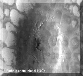
The pore in this 50 µm (0.002") electroless nickel coating reaches all way down to the steel bottom (the lower (darker) BSE signal indicates iron in the middle of the pore). Fine cracks can be distinguished as well around the pinhole bottom. |
 |
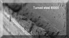
This fine-turned steel-52 axle demonstrates the corrosion protection limiting issue for metal platers. Turning and similar operations are actually tearing operations, which can cause scaled micro-structures. These micro-scales can impart a pinhole problem to galvanic processes. Surface refinement can reduce this problem. |
 |
 |
.

Lunac 1 coatings are able to deliver crack-free faultless coatings on machine parts.
The substrate needs to be ground smoothly and free of serious material defects
(the fine lines are polish lines)